
:format(url)/cloudfront-us-east-1.images.arcpublishing.com/lescoopsdelinformation/C3VYAWOPWFGBFKDZOWF6VNLY54.jpg)


The University of Ottawa, in collaboration with national and international partners, has achieved world number one status by manufacturing back-contact microphotovoltaics. This innovative breakthrough could lead to increased miniaturization in electronic devices.
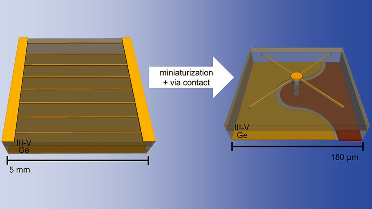
The cells, which are twice the size of a strand of hair, offer significant advantages over traditional solar technologies. It reduces electrode shadowing by 95% and can reduce energy production costs by up to three times.
The manufacturing process of micrometer photovoltaics involved a partnership between…University of Ottawa,l’University of Sherbrooke in Quebec and the Microelectronics Technologies Laboratory in Grenoble (Limited time), in France.
” These micrometer photovoltaics have remarkable features, including extremely small size and significantly reduced shading. These properties lend themselves to a variety of applications, from the densification of electronic devices to areas such as solar cells, lightweight nuclear batteries for space exploration, and the miniaturization of communications and Internet of Things devices. “, says Karen Henzer, vice provost for research and holder of the University Research Chair in Energy Photonic Devices in the College of Engineering.
Huge potential
” This technological breakthrough promises great benefits to society. Cheaper and more powerful solar cells will help accelerate the energy transition. Lightweight nuclear batteries will facilitate space exploration, and device miniaturization will help the Internet of Things grow and lead to more powerful computers and smartphones. », adds Mathieu de La Fontaine, a postdoctoral researcher at the University of Ottawa and part-time professor of physics.
” The development of these first back-contact micrometer photovoltaics is a crucial step in the miniaturization of electronic devices “, He specifies.

(a) Schematics of a 2D electronic circuit on an epiwafer III-V wafer and a 3D electronic circuit on two Epiwafer III-V sheets glued together and interconnected by pass-through substrate.
(b) Photothermal cell with 2D planar connections and 3D interconnections using TSVs.
Towards a carbon neutral economy
” Semiconductors are essential in the transition to a carbon neutral economy. This project is one of the many research initiatives we are undertaking at the College of Engineering to achieve our societal goals “, comments Karen Henzer.
Semiconductors fall into three of the five research areas in the Faculty of Engineering, namely Information Technology, Photonics and Emerging Materials, and two of the four strategic research areas at the University of Ottawa, namely Creating a Sustainable Environment and Shaping the Digital World.

(A-C) Schematic illustration of (A) a standard strip and grid-line small solar cell, (B) a through-substrate small solar cell (TSV), and (C) a small through-substrate-contact solar cell (X-TSV). ) from front (left) and back (right).
(d) The table compares the shading factor for each design. The shading factors for metal-shell Si solar cells (MWT) and efficiencies were taken from the literature18,19,20,21,22,25,27 and this work.
Synthetic
This international partnership between Canada and France demonstrates the importance of innovation and research in small manufacturing, paving the way for a future where technology is more powerful and accessible than ever before. It also represents a historical milestone in the development of the global scientific and technological scene.
For better understanding
What are micrometer back contact photovoltaics?
These are micrometer-sized solar cells, twice as thick as a strand of hair, and have been manufactured for the first time by the University of Ottawa and its partners. They offer significant advantages over traditional solar technologies.
What are the characteristics of these cells?
It reduces electrode shadowing by 95% and can reduce energy production costs by up to three times.
Who are the partners in this project?
The project includes a partnership between the University of Ottawa, the University of Sherbrooke in Quebec, and the Microelectronics Technologies Laboratory in Grenoble, France.
What are the potential applications of these cells?
They lend themselves to a variety of applications, from the densification of electronic devices to areas such as solar cells, lightweight nuclear batteries for space exploration, and the miniaturization of communications and Internet of Things devices.
What is the impact of this achievement on society?
Cheaper and more powerful solar cells will help accelerate the energy transition. Lightweight nuclear batteries will facilitate space exploration, and device miniaturization will contribute to the growth of the Internet of Things and lead to more powerful computers and smartphones.
Key lessons
| Teachings |
|---|
| 1. First micrometer fabrication of back contact photovoltaics |
| 2. 95% reduction in shadowing caused by the electrode |
| 3. The possibility of reducing energy production costs by up to three times |
| 4. Partnership between the University of Ottawa, the University of Sherbrooke and the Laboratory of Microelectronics Technologies |
| 5. Potential applications in densification of electronic devices, solar cells, lightweight nuclear batteries for space exploration, miniaturization of communications devices and the Internet of Things |
| 6. Contributing to accelerating the transition to energy, space exploration, and the growth of the Internet of Things |
| 7. The importance of semiconductors in the transition to a carbon neutral economy |
| 8. Inclusion of semiconductors in three of the five research areas in the Faculty of Engineering at the University of Ottawa |
| 9. Explain the importance of innovation and research in the field of precision manufacturing |
| 10. It represents a historical milestone in the development of the global scientific and technological scene |
References
The fabrication of these micrometer photovoltaics is described in detail in the journal Cell Reports Physical Sciences Under the title “Three-dimensional junctions of III-V semiconductor heterostructures for miniaturized power devices“.
[ Rédaction ]

“Hardcore beer fanatic. Falls down a lot. Professional coffee fan. Music ninja.”
More Stories
57,000 neurons in 1 cubic mm
Quality fishing and many adventures are in store for Lac Blanc
Unstoppable attack on VPNs?